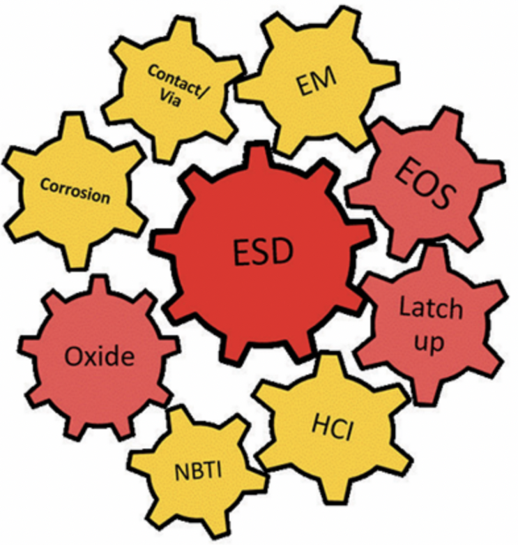
반도체 Very Large Scale Integration (VLSI) 설계 세계에서, Process Design Kit (PDK)는 silicon fabrication과 integrated circuit 설계 사이의 근본적인 다리 역할을 합니다. 레고 블록 모듈이라고 보면 좋을 것 같아요.
칩 설계 엔지니어들은 이 레고블록으로 건물을 만들구요. Technology Computer-Aided Design (TCAD), SPICE modeling, 그리고 Device characterization까지 보고, Post silicon validation 후에 Calibration과 Silicon re-charac은 어떻게 진행되는지..
PDK version 1.0, 2.0 3.0 어떻게 바뀌어나가는건지... 살펴봅시다.
PDK란 무엇인가? 생성 flow에 대해 살펴보기 전에, PDK가 무엇인지 명확히 이해해 봅시다.
Process Design Kit은 semiconductor foundr...
원문 링크 : PDK란? Process Design Kit